Zhejiang and RMIT researchers embed spectral sensing into imaging hardware
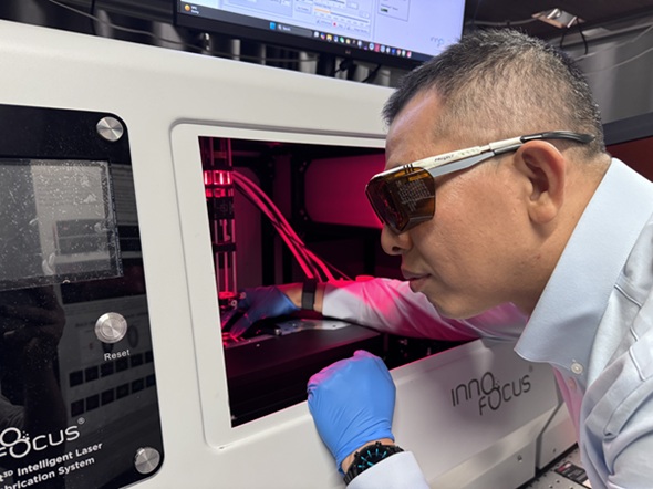
Researchers from Zhejiang University and RMIT University have developed a compact imaging chip that integrates spectral analysis directly into hardware using microscopic light-sorting structures. This prototype, demonstrated with commercial sensors, enables on-chip spectral sensing without the need for bulky external laboratory equipment.
Key Takeaways
- Researchers fabricated tiny spiral-shaped light-sorting structures 1,000 times smaller than a human hair inside transparent materials.
- Integrated prototype demonstrates real-time spectral sensing using commercial image sensors across visible and near-infrared wavelengths.
- Hardware-based approach eliminates the need for bulky external laboratory equipment or specialized post-processing software for material identification.
- Microscale structures remain largely unaffected by viewing angles, overcoming a primary limitation of previous miniaturized optical technologies.
Why It Matters
This development moves spectral imaging from specialized laboratories directly into the sensor stack, potentially reducing the hardware footprint for advanced machine vision. By sorting light physically at the sensor level rather than relying on software-heavy reconstruction, this approach could streamline material identification in automated sorting and environmental monitoring. For the streaming and video ecosystem, this signals a shift toward "hyperspectral-ready" professional cameras that can distinguish authenticity and surface textures beyond standard RGB capabilities. Watch for follow-up testing on the scalability of the ultrafast laser fabrication process used to create these microscale spirals.
Additional Context
The miniaturization of hyperspectral imaging (HSI) has emerged as a central focus for sensor manufacturers in 2026. Per Fortune Business Insights, the global HSI market is projected to reach approximately $292.5 million by 2026, driven by a 12% annual growth rate. This expansion is largely attributed to the increasing demand for portable spectral intelligence in industrial automation and remote sensing. While traditional pushbroom and line-scan sensors currently dominate nearly 60% of the market, the emergence of integrated snapshot-style chips, like the Zhejiang-RMIT prototype, aims to lower the high equipment costs and processing complexity previously associated with the field. Industrial sensor vendors are increasingly moving toward "full-stack" multi-modal architectures to support edge computing. Per EE Times (February 2026), startups like AlpsenTek are already working to fuse conventional CMOS frames with event-based and spectral sensing at the pixel level. This broader trend targets the reduction of redundant data streams while providing AI models with richer physical context. Furthermore, research from Aalto University in January 2025 demonstrated a 5-micrometer spectral sensor capable of identifying materials with 0.2-nanometer accuracy, underscoring a competitive race to bring laboratory-grade spectroscopy into hand-held and wearable consumer devices. In the medical and clinical sectors, these compact sensors are being optimized for "chip-on-tip" endoscopic applications. Per Aivon (March 2026), advanced imaging stacks that incorporate spectral techniques are now being used to improve real-time tissue characterization and surgical precision. As these technologies migrate into high-end production hardware, they allow for automated quality control systems that can detect surface contaminants or material fatigue at the point of capture, rather than through delayed post-processing.
Read full article at photonics.com