

AMD integrated on-package memory simplifies professional video and edge streaming designs
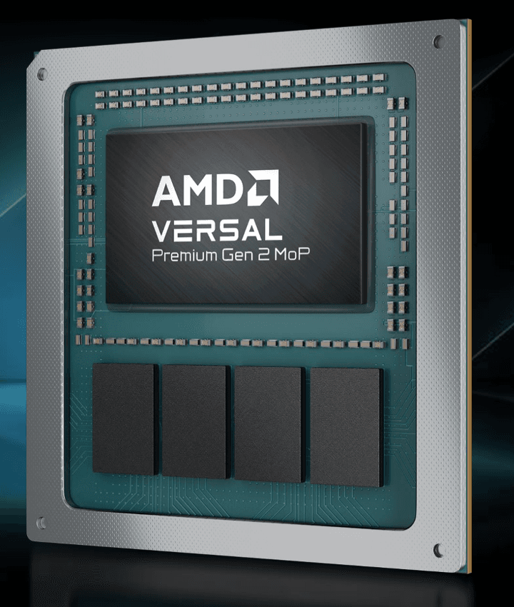
AMD has unveiled the Versal Premium Gen 2 Memory on Package (MoP) adaptive SoC, which integrates 32 GB of LPDDR5X memory directly into the package. Targeting professional video processing and edge streaming applications, the device aims to provide high bandwidth and compact form factors for long-lifecycle industrial and embedded deployments.
Key Takeaways
- Integrated 32 GB LPDDR5X memory achieves up to 288 GB/s bandwidth, removing the need for external DRAM routing.
- On-package design yields 60% board-area savings compared to discrete-memory implementations, enabling more compact form factors like 3U VPX.
- The platform guarantees 15-plus years of availability and supports industrial temperatures from -40°C to 110°C.
- Hardware support for PCIe Gen6 and CXL 3.1 enables 64 Gb/s data movement for memory pooling and expansion.
- Sampling is scheduled for late 2026, with volume production shipments expected in the second half of 2027.
Why It Matters
By moving memory onto the SoC package, AMD removes the complex high-speed routing and validation cycles that delay time-to-market for professional video and networking hardware. This strategy positions LPDDR5X-based on-package memory as a pragmatic alternative to HBM for edge applications where long lifecycles and industrial thermal ranges are mandatory, but data center-grade HBM supply is volatile. For the streaming ecosystem, this facilitates denser, more efficient edge-processing nodes for real-time video enhancement and AI-assisted transcoding. Industry observers should watch for rival FPGA vendors to adopt similar memory-on-package architectures as HBM prices and availability remain concentrated among data center hyper-scalers.
Additional Context
The shift toward integrated memory on package (MoP) reflects a broader industry response to the ‘memory wall’ and the rising costs of High Bandwidth Memory (HBM). Per Wccftech in June 2026, AMD’s decision to use LPDDR5X for this series—rather than the HBM modules common in high-end data center GPUs—is a strategic pivot to insulate long-lifecycle industrial customers from the volatile supply and pricing of the HBM market. While HBM3E can provide over 1.2 TB/s of bandwidth, it typically requires active cooling and follows short product refresh cycles that do not align with the 15-year support required for telecom and defense infrastructure.
Technically, this release bridges the gap between traditional FPGAs and specialized AI accelerators. According to analysis from StorageReview in June 2026, combining in-package memory with hard IP for PCIe 6.0 and CXL 3.1 allows these chips to function as high-efficiency hubs for distributed AI. By pairing Versal Gen 2 with AMD Epyc CPUs, architects can use CXL 3.1 to pool memory across multiple devices, effectively scaling capacity beyond the initial 32 GB MoP limit while maintaining the low-latency performance of the local LPDDR5X interface.
Competitively, AMD’s move intensifies the architecture battle with Intel’s Programmable Solutions Group (Altera). While Intel’s Agilex series has historically led on raw HBM2e bandwidth for data center workloads, per FPGainsights in June 2026, AMD is focusing on the edge-AI and embedded sectors where thermal-to-performance ratios and board-space constraints are the primary design hurdles. This latest Versal iteration specifically enables standard Enterprise and Datacenter Standard Form Factors (EDSFF) that were previously difficult to design with discrete memory layouts due to signal integrity challenges and routing complexity.
Read full article at jonpeddie.com
Enjoy our coverage?
Add StreamingMeme as a preferred source on Google to see more of our streaming news at the top of your Search results.
Add as preferred source