

SK hynix deploys EUV technology to anchor future high-bandwidth memory
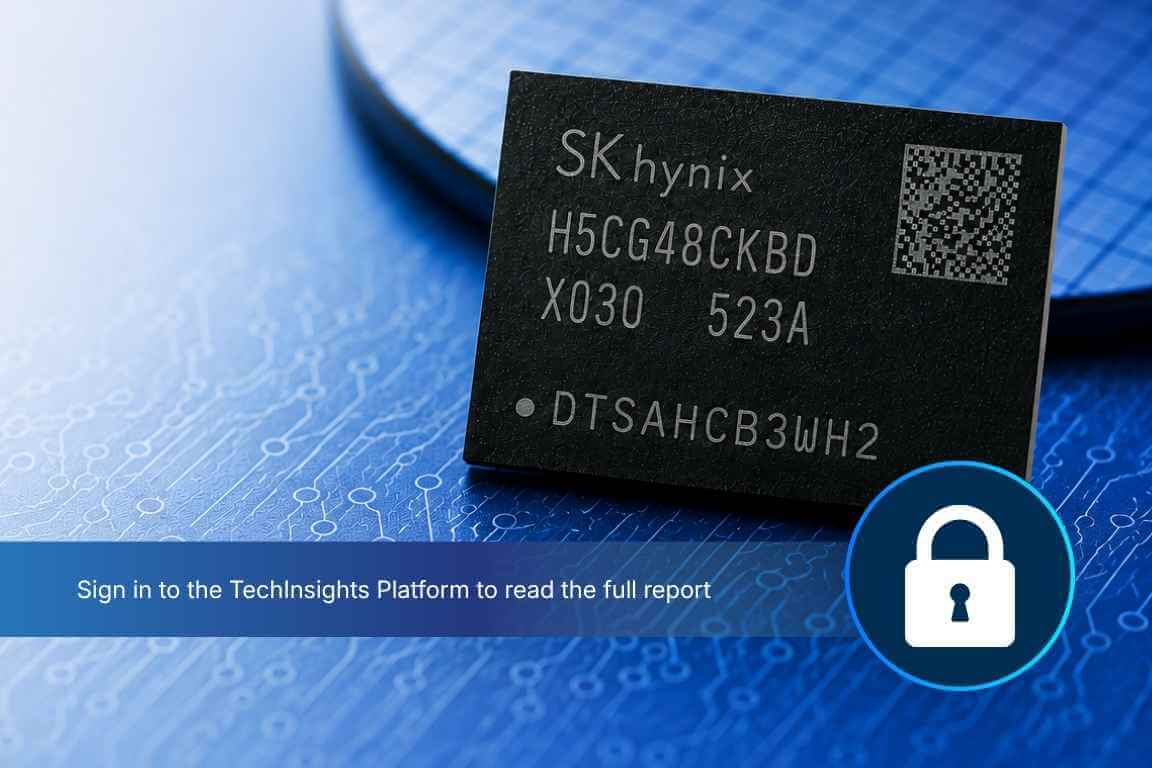
TechInsights' analysis of SK Hynix's D1c DRAM confirms its use of EUV technology, which is pivotal for advanced memory production. This technological advancement is crucial for the development of upcoming HBM4e and HBM5 memory generations. These high-bandwidth memory solutions are essential for high-performance computing, including applications in streaming infrastructure.
Key Takeaways
- Confirmed use of EUV lithography in D1c DRAM enables further feature-size reductions and improved yield optimization.
- Integrated EUV technology serves as the manufacturing foundation for future HBM4e, HBM5, and LPDDR6 memory products.
- Higher memory density and bandwidth from the 10nm-class D1c node are categorized as critical for next-generation data center applications.
- Analysis identified the SK hynix H5CG48CKBD-X030 16Gb DDR5 DRAM as a primary device utilizing this advanced node.
Why It Matters
The shift to EUV for D1c DRAM marks a critical point where memory physics must evolve to support the massive throughput demands of modern media delivery and generative AI. This directly affects streaming by securing the roadmap for HBM5, which will drive the high-resolution encoding and real-time personalization engines at the edge and in the core. As streaming platforms transition to 8K and low-latency interactive video, the bandwidth provided by EUV-node memory becomes the primary hardware bottleneck. Watch for SK hynix's HBM4e mass production schedule in late 2026, as any delay would disrupt the launch cycles of next-generation server GPUs used in video processing.
Additional Context
The acceleration of EUV-based memory production reflects an industry-wide scramble to solve what analysts call the "memory wall." Per TrendForce in June 2026, SK hynix recently unveiled its iHBM solution, which integrates silicon-based cooling elements directly into the memory package to reduce thermal resistance by 30%. This innovation is designed to mitigate the intense heat generated by high-density stacking in HBM4e and HBM5, where power consumption for AI server GPUs is now trending toward 1,000W per chip. To support this infrastructure, the South Korean government announced on June 2, 2026, that it would streamline EUV equipment approval processes, reducing installation lead times from 34 days to just nine.
Simultaneous to these technical shifts, the economic landscape of memory has moved into what Morgan Stanley calls "Chipflation." Reporting from June 2026 indicates that SK hynix has already sold out its entire DRAM and HBM production capacity through the end of the year, driven largely by a multi-year co-development deal with NVIDIA for the Vera Rubin platform. This surge in high-margin HBM demand is creating a structural squeeze for standard enterprise hardware. According to a June 2026 coalition letter from NCTA and ACA Connects, surging memory prices are already increasing the cost of telecommunications and streaming infrastructure, as manufacturers prioritize HBM for AI over the standard DRAM used in traditional networking and server equipment.
Read full article at techinsights.com
Enjoy our coverage?
Add StreamingMeme as a preferred source on Google to see more of our streaming news at the top of your Search results.
Add as preferred source