

Samsung targets 1.4nm+ mass production by 2030 to challenge TSMC
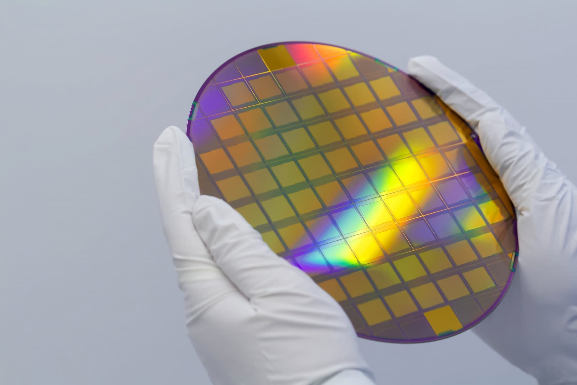
Samsung has announced its 1.4nm+ process node for 2030, alongside an updated roadmap for 2nm gate-all-around (GAA) technology. The company is adopting Design and Process Integration Optimization (DTCO) techniques to improve power and performance for high-performance computing and AI applications.
Key Takeaways
- Samsung’s SF1.4+ node is scheduled for 2030, one year after the primary 1.4nm process begins mass production in 2029.
- DTCO techniques applied to 2nm nodes yielded a 26% power improvement and 15% clock speed boost, which will be critical for sub-2nm scaling.
- Mass production for the third-generation 2nm node (SF2P+) and the AI-optimized SF2X is targeted for the 2027 to 2028 window.
- Enhanced focus on stabilizing 2nm yields follows reports that Apple may seek sub-2nm supply from multiple foundries to avoid capacity constraints.
Why It Matters
Samsung is positioning its roadmap to break TSMC's dominance in the advanced node market, particularly as AI-driven demand for flagship mobile and data center silicon stays high. By providing a credible 1.4nm-class alternative by 2029, Samsung aims to secure orders from hyperscalers and Apple, which is reportedly exploring supply diversification for future M-series chips. For the streaming ecosystem, these hardware gains directly impact server-side encoding efficiency and the performance of local AI-driven video processing on edge devices. Industry watchers should monitor Samsung's Taylor, Texas fab progress as the primary indicator for 2nm and 1.4nm volume readiness.
Additional Context
The race for sub-2nm leadership is accelerating as TSMC and Intel firm up their own angstrom-class targets. Per Tom's Hardware (June 2026), TSMC remains on track for mass production of its A14 (1.4nm) process in 2028, maintaining a one-year lead over Samsung. Meanwhile, Intel is leveraging its early adoption of High-NA EUV lithography, with its 14A node slated for risk production in 2028 and volume manufacturing in 2029. This creates a rare three-way competition for the industry's most advanced transistors at the end of the decade.
Yield stability remains the primary hurdle for Samsung. Recent industry tracking by Chosun Daily (February 2026) indicated that Samsung reached a 70% yield milestone for its SF2P node, a significant recovery after struggles with early 3nm GAA production. This stabilization proved critical for securing a $16.5 billion contract with Tesla, per PhoneArena (June 2026), providing the financial foundation to resume development of the SF1.4 and SF1.4+ schedules.
Strategic pressure from primary customers like Apple is a major driver of this roadmap. According to The Bell (July 2026), Apple is actively evaluating Intel’s 18A-P and 14A nodes for future M7-series chips specifically to mitigate supply risks associated with TSMC. By formalizing the SF1.4+ roadmap, Samsung is signaling to major fabless designers that it can offer performance enhancements through DTCO without the massive IP migration costs typically associated with moving to a completely new lithography generation.
Read full article at wccftech.com
Enjoy our coverage?
Add StreamingMeme as a preferred source on Google to see more of our streaming news at the top of your Search results.
Add as preferred source