

NVIDIA launches NVLink 6 to boost AI inference and throughput
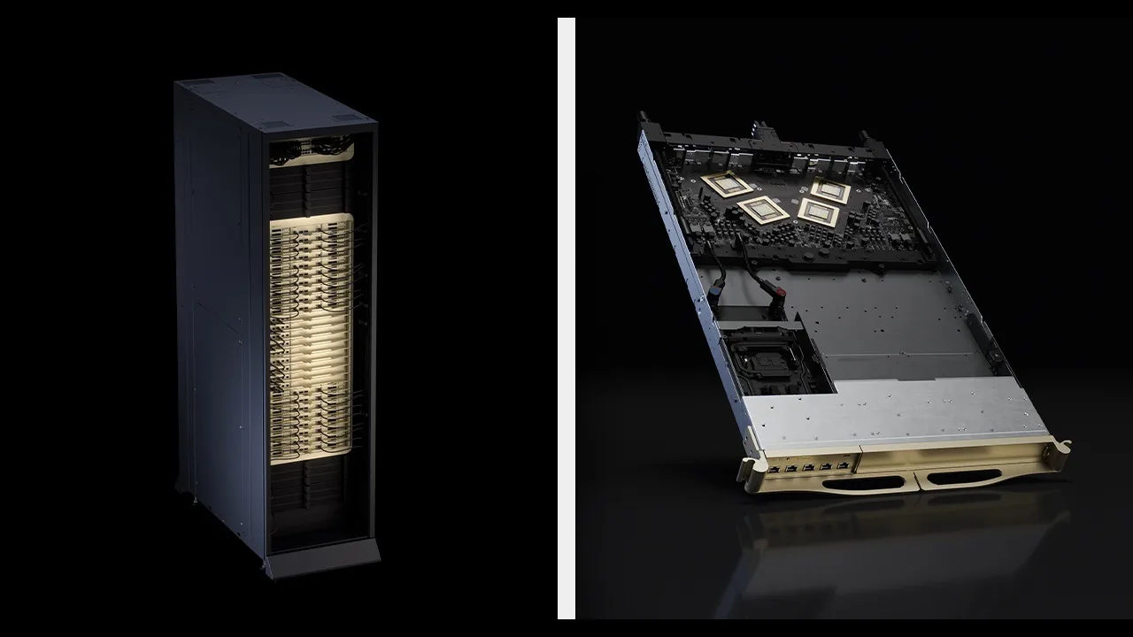
NVIDIA has released technical details regarding its sixth-generation NVLink and NVLink 6 Switch, a scale-up networking fabric designed for high-performance AI data centers. The vendor claims the architecture improves inference and training performance, offering up to 2.3x higher decode throughput for large-model workloads compared to standard Ethernet.
Key Takeaways
- Sixth-generation NVLink provides 3.6 TB/s of bidirectional GPU-to-GPU bandwidth and 260 TB/s at the rack level.
- NVLink 6 delivers 2.3x higher decode throughput for DeepSeek-R1 and Qwen 235B models versus off-the-shelf Ethernet.
- Integrated support for SHARP in-network compute offloads collective operations to reduce communication overhead in mixture-of-experts (MoE) models.
- New management and resiliency features enable production AI factory uptime through rack-level fault management.
Why It Matters
The shift from training to large-scale real-time inference requires networking that enables multiple GPUs to work as a single logical unit. This launch reinforces NVIDIA's strategy of total system co-design, making the interconnect as vital as the processor for token-per-watt efficiency. By significantly outperforming standard Ethernet in low-latency all-to-all communication, NVIDIA deepens its competitive moat against generic hardware and standard networking fabrics. For operators, this represents a trade-off between the better performance of a proprietary stack and the lower costs of open standards. Watch for whether hyperscalers accelerate their custom silicon networking projects specifically to address this 2.3x performance gap.
Additional Context
The rollout of NVLink 6 arrives as NVIDIA's Vera Rubin platform succeeds the Blackwell architecture to address the demands of agentic AI. Per Bizon-Tech in April 2026, the Vera Rubin VR200 GPU features 288GB of HBM4 and was built to natively support 6th-generation NVLink. This integration is central to NVIDIA's 'AI factory' vision, where data center networking is treated as an extension of the GPU rather than a separate silo. SiliconAngle reported in July 2026 that this co-design approach currently places NVIDIA materially ahead of competitors who rely on standard Ethernet protocols, which suffer from higher latency and lower message rates.
While NVIDIA maintains approximately 80% of the AI accelerator market, competitors are increasingly targeting the interconnect gap. According to Silicon Analysts in April 2026, AMD’s MI350X offers higher HBM capacity than NVIDIA’s B200, yet trails significantly in interconnect speed, with Infinity Fabric providing roughly 128 GB/s per pair compared to NVLink’s much higher throughput. This disparity impacts real-world multi-GPU scaling efficiency, particularly for trillion-parameter models that rely on expert parallelism.
Faced with NVIDIA's proprietary lock-in, several major players are pivoting to custom silicon. Per Seeking Alpha in July 2026, Broadcom’s AI semiconductor revenue is projected to reach $56 billion for the year, driven by multi-year partnerships with OpenAI, Meta, and Google to develop custom ASICs. Simultaneously, Cerebras has gained traction with its wafer-scale technology, securing a $20 billion commitment from OpenAI per reports in June 2026. These developments suggest that while NVIDIA’s NVLink 6 sets a high technical bar for performance, the industry is bifurcating between high-end proprietary ecosystems and cost-optimized custom silicon.
Read full article at developer.nvidia.com
Enjoy our coverage?
Add StreamingMeme as a preferred source on Google to see more of our streaming news at the top of your Search results.
Add as preferred source