

NVIDIA detail's 256Gb/s DWDM link to solve AI interconnect bottlenecks
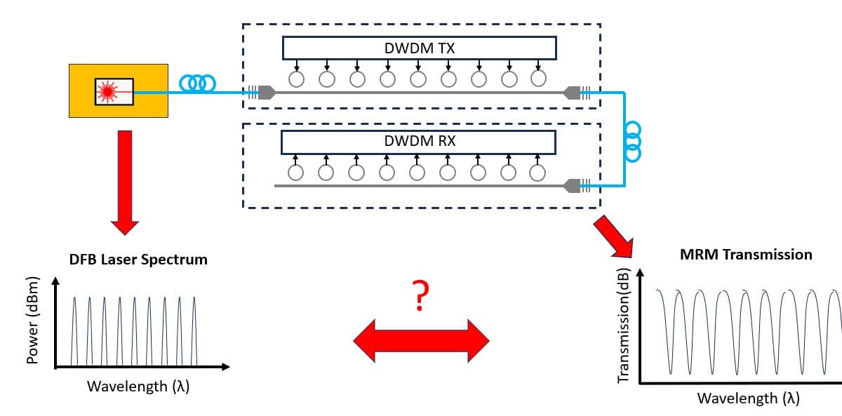
This technical analysis details the architecture of Nvidia's 256Gb/s dense-wave division multiplexing (DWDM) optical link, including its use of microring modulators and injection-locked oscillators. The article explains how co-packaged optical systems leverage these components to address energy efficiency, latency, and signal synchronization challenges in advanced data transmission.
Key Takeaways
- DWDM link achieves 256Gb/s per fiber by multiplexing eight 32Gb/s data channels with a 16GHz forward clock lane.
- Architecture employs an injection-locked oscillator (ILO)-based bandpass filter to mitigate random jitter from transimpedance amplifiers.
- The 3D-stacked design integrates a 7nm electronic integrated circuit (EIC) with a 65nm photonic integrated circuit (PIC).
- Microring modulators serve as ultra-compact on-off switches, though they require integrated thermal tuning loops to manage temperature sensitivity.
Why It Matters
NVIDIA's shift toward DWDM and co-packaged optics (CPO) represents a fundamental pivot in data center hardware to overcome the 'power wall' of traditional copper interconnects. By moving optical engines directly onto the chip package, NVIDIA can drastically reduce signal energy dissipation while maintaining the massive bandwidth required for distributed AI workloads. This technical implementation signals a move away from pluggable transceivers toward integrated silicon photonics as a standard for high-density compute clusters. For the streaming industry, these infrastructure gains directly support the back-end scale needed for real-time generative video and global-scale low-latency distribution. Watch for initial commercial deployment in NVIDIA’s Spectrum-X and Quantum-X switches throughout late 2026.
Additional Context
NVIDIA is rapidly formalizing its optical supply chain to support the commercial rollout of these technologies. In March 2026, the company announced multiyear strategic partnerships with Lumentum and Coherent, including a $2 billion investment in each to secure future manufacturing capacity and research for advanced laser components (per NVIDIA, March 2026). These agreements include multibillion-dollar purchase commitments, ensuring that the critical external laser sources required for DWDM systems remain stable as AI 'factories' grow in complexity and volume.
The deployment of this technology is closely tied to TSMC’s COUPE (Compact Universal Photonic Engine) platform, which utilizes 3D hybrid bonding—specifically SoIC-X—to tether compute and photonic dies on a single substrate. According to external reporting from ECTC 2026, this 'bumpless' interconnect technology reduces parasitic capacitance and impedance mismatch, allowing the system to achieve energy efficiency figures as low as 2.6 pJ/bit (per SimpleTechTrend, March 2026). This level of efficiency is nearly 40% better than existing pluggable transceiver architectures.
Broader industry movements also point toward the standardization of these interfaces. The launch of the Optical Computing Interconnect (OCI) MSA in early 2026—backed by NVIDIA, Broadcom, and Microsoft—aims to establish high-volume standards for 200Gb/s bidirectional links. While Broadcom continues to emphasize Mach-Zehnder modulators for scale-out Ethernet switching, NVIDIA’s commitment to microring modulators suggests a distinct focus on maximizing edge density and power efficiency for internal cluster scale-up (per IDTechEx, March 2026).
Read full article at chadw.substack.com
Enjoy our coverage?
Add StreamingMeme as a preferred source on Google to see more of our streaming news at the top of your Search results.
Add as preferred source