

Intel EMIB-T breaks packaging limits for ultra-large AI and HPC chips
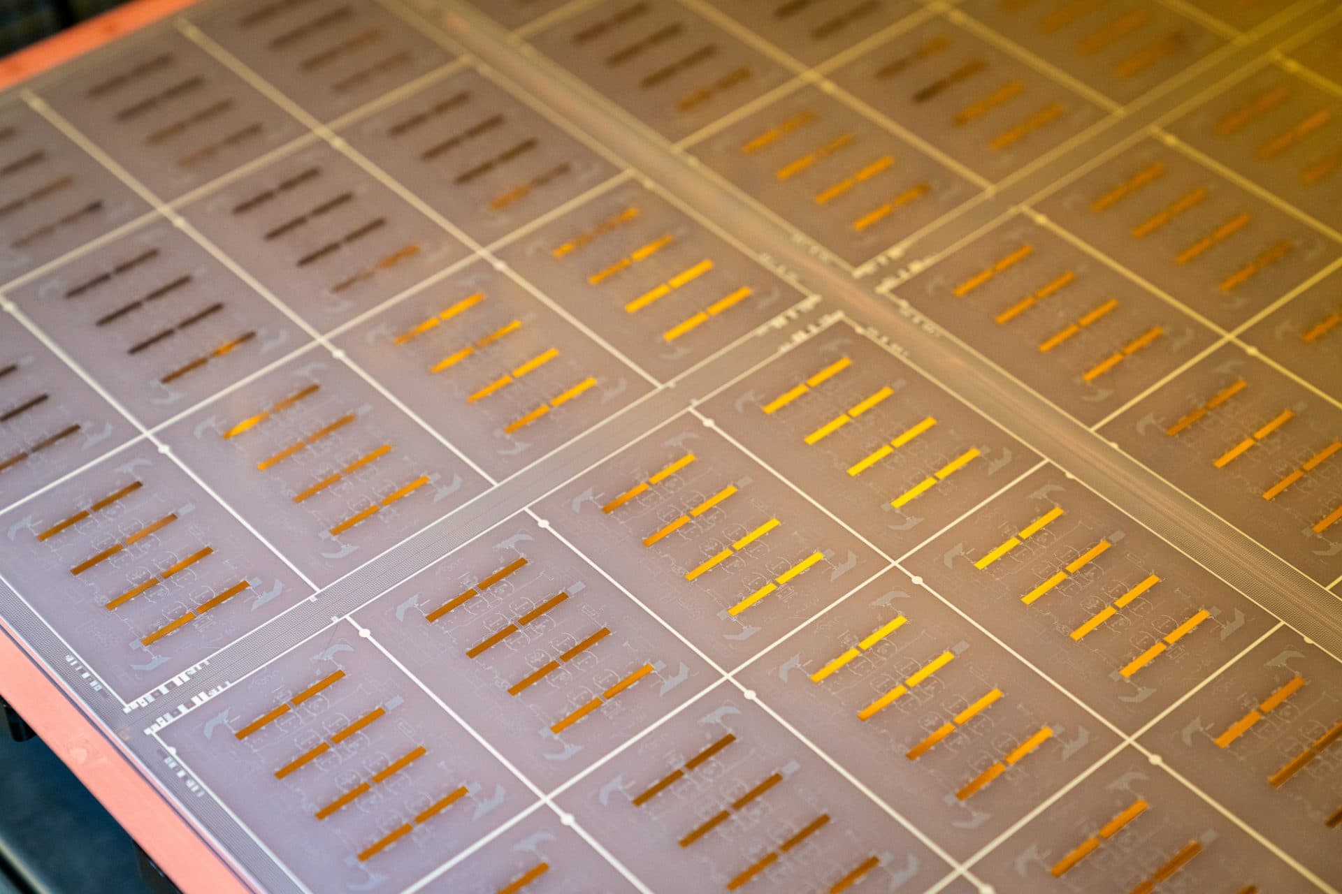
Intel demonstrated its new EMIB-T advanced packaging technology at ECTC, designed for ultra-large die complexes and high-bandwidth HBM4e memory integration. The technology aims to provide a scalable, high-performance solution for the next generation of AI and HPC hardware, directly addressing current chip scaling and power limitations.
Key Takeaways
- EMIB-T technology enables high-speed signaling exceeding 12 Gb/s for HBM4e memory integration
- Package form factors can scale to ultra-large 240 x 240 mm dimensions for hyper-large AI systems
- Architecture supports disaggregating large systems into chiplets while maintaining low energy overhead, featuring SRAM bandwidth of 265 GB/s/mm²
- Verified customers for Intel’s advanced packaging include Google, NVIDIA, and the Tesla-linked TeraFab project
Why It Matters
The introduction of EMIB-T directly addresses the primary bottleneck in the AI silicon supply chain: the availability of high-density 2.5D packaging. By moving beyond the physical reticle limits of standard lithography, Intel provides a viable domestic alternative to TSMC’s CoWoS, which currently faces severe capacity constraints. For streaming infrastructure providers, this means the potential for more efficient, high-bandwidth server clusters capable of handling exponentially larger transcoding and generative AI workloads. Watch for Intel's certification of 35 µm bump pitches by the end of 2026, which will signal the platform's readiness for commercial-volume HPC deployments.
Additional Context
Intel’s pivot toward advanced packaging comes as the industry faces a structural deficit in 2.5D assembly capacity. Per Silicon Analysts in June 2026, TSMC’s CoWoS (Chip-on-Wafer-on-Substrate) lines remain fully booked through 2027, with lead times stretching between 52 and 78 weeks. This bottleneck has forced major hyperscalers to seek alternatives, as NVIDIA reportedly secured 60% of TSMC's total 2026 advanced packaging output to support its Blackwell and Rubin architectures. Intel’s ability to offer a scalable alternative through its Arizona-based Assembly and Test factories is a critical component of its foundry turnaround strategy, with CFO David Zinsner noting in early 2026 that individual packaging contracts could exceed $1 billion in revenue.
Simultaneously, Intel is evolving the materials science underlying these interconnects. At NEPCON Japan in January 2026, the company debuted its first glass substrate samples, which feature a 10-2-10 vertical layer architecture designed to mitigate the 'warpage wall' that limits traditional organic substrates. Per TrendForce in May 2026, volume production for these glass-based solutions is slated for the Rio Rancho facility in New Mexico. By integrating EMIB bridges directly into glass, Intel claims it can double the silicon area of current accelerators, positioning the company roughly 18 months ahead of competitor glass-based solutions expected to reach panel-level scale by 2027.
Customer momentum for these technologies is intensifying. Per The Information in June 2026, Google has already committed to ordering over three million custom Tensor Processing Units (TPUs) from Intel Foundry for 2028 production, a deal heavily dependent on Intel's advanced packaging capabilities. Furthermore, NVIDIA has begun running early-stage trials on Intel’s 18A process to test the fusion of four graphics chips into a single module. These commitments, alongside the Tesla-linked TeraFab partnership announced in April 2026, suggest that Intel is successfully leveraging its packaging head-start to secure anchor clients as domestic semiconductor manufacturing becomes a priority for national security as well as commercial scalability.
Read full article at wccftech.com
Enjoy our coverage?
Add StreamingMeme as a preferred source on Google to see more of our streaming news at the top of your Search results.
Add as preferred source