

AMD partners with NeoLogic to bypass the industry’s SRAM scaling wall
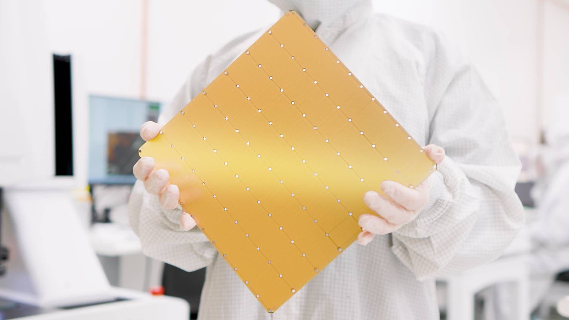
AMD has partnered with semiconductor startup NeoLogic to integrate high-speed, low-power SRAM alternative architecture into its processors. This strategic move aims to reduce chip footprint and costs for AMD's EPYC CPUs and Instinct accelerators, providing a capital-efficient alternative to the large-scale acquisitions pursued by competitors like Nvidia.
Key Takeaways
- NeoLogic technology claims to reduce chip area by 40% and power consumption by 50% compared to standard CMOS designs.
- Integrated IP targets memory bottlenecks in AMD’s EPYC CPUs and Instinct AI accelerators at advanced process nodes.
- The partnership contrasts with Nvidia’s $20 billion infrastructure spend, including the acquisitions of Mellanox and Run:ai.
- Strategic move enables AMD to pack higher compute density into smaller silicon dies without traditional SRAM scaling constraints.
Why It Matters
The deal signals a shift toward specialized architectural IP as a survival tactic for chipmakers facing the end of physical transistor scaling. As traditional SRAM fails to shrink alongside logic at 3nm and below, on-chip memory takes up a disproportionate percentage of the die, driving up manufacturing costs for GPU/CPU providers. For the streaming and cloud infrastructure sectors, this directly impacts the cost-to-performance ratio of the high-density servers required for transcoding and AI-driven content personalization. By lowering the physical footprint and power overhead of its caches, AMD can pressure Nvidia on both price and rack-level density. Watch for whether this architecture appears in the 2026 Venice EPYC lineup.
Additional Context
The semiconductor industry is currently grappling with a structural scaling problem where standard memory cells (SRAM) are no longer shrinking in proportion to logic gates. Per Tom's Hardware in late 2024, TSMC’s N3E (3nm) process provided virtually no density advantage for SRAM over the older 5nm node, leading to massive chips where memory blocks consume excessive silicon area. NeoLogic's 'Quasi-CMOS' approach, which reduces transistor counts and simplifies logic gates, is designed to break this bottleneck. Per TechRadar Pro in August 2025, the startup’s technology allows single-stage gates to handle up to 32 inputs, significantly shortening the critical path of data flow within the processor. This architectural pivot arrives just as AMD scales its enterprise AI footprint. At its 'Advancing AI' event in July 2026, AMD officially debuted the 6th Generation EPYC 'Venice' CPUs and Instinct MI400 accelerators. Per AMD corporate materials from July 2026, the company is now shipping 'Helios' rack-scale systems to major partners like Microsoft and Oracle, claiming up to 30% more tokens per dollar for AI inference compared to rival solutions. While Nvidia has spent heavily on software-driven optimization through its $700 million acquisition of Run:ai (per VentureBeat, December 2024), AMD’s deal with NeoLogic focuses on the physics of the silicon itself. The technical stakes are high as the industry moves toward 2nm production. Per Third Bridge via Substack in January 2026, TSMC’s 3nm capacity is already oversubscribed by Nvidia and Apple, forcing secondary players to find architectural efficiencies to remain competitive on cost. If NeoLogic's design yields the promised 40% area savings, AMD could potentially offset the rising wafer costs associated with ultra-advanced lithography, maintaining its share of the server CPU revenue market, which reached 46.2% in the first quarter of 2026 according to vaysinfotech.
Read full article at techradar.com
Enjoy our coverage?
Add StreamingMeme as a preferred source on Google to see more of our streaming news at the top of your Search results.
Add as preferred source